• Proximity-induced magnetic ordering in topological insulators
• Dissipation-less transport in topological edge states
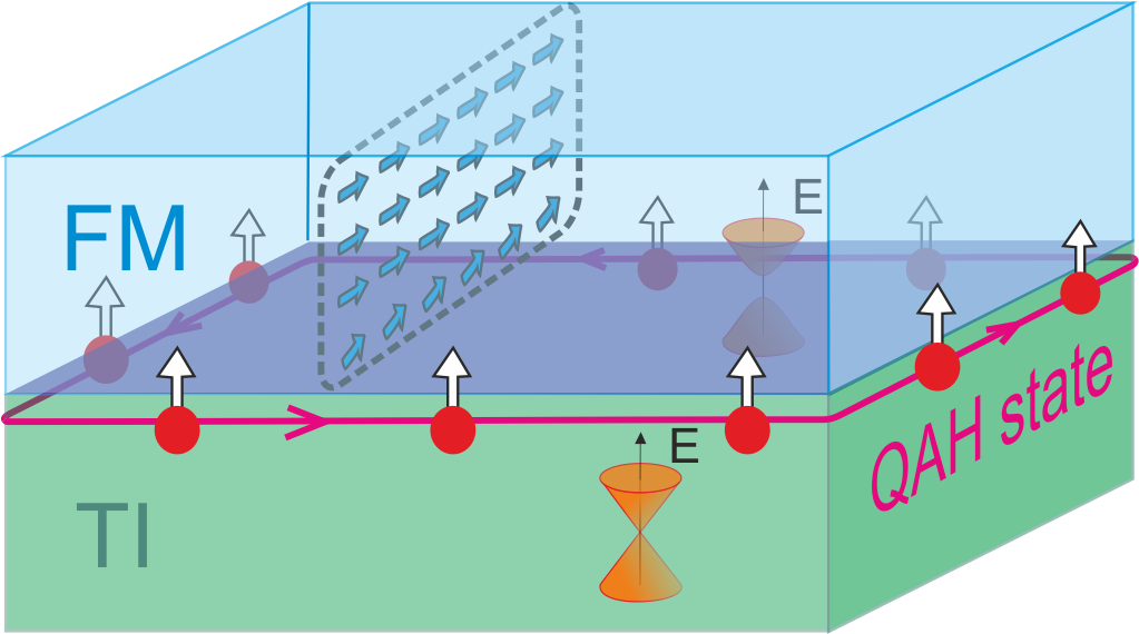
• Proximity-induced magnetic ordering in topological insulators
• Dissipation-less transport in topological edge states
• p-n junctions, TI nanowires, electrical and optical excitation of spin-polarized currents
• 2D transport - GaAs/AlGaAs-based 2-dimensional electron gases (2DEGs), Anderson localization
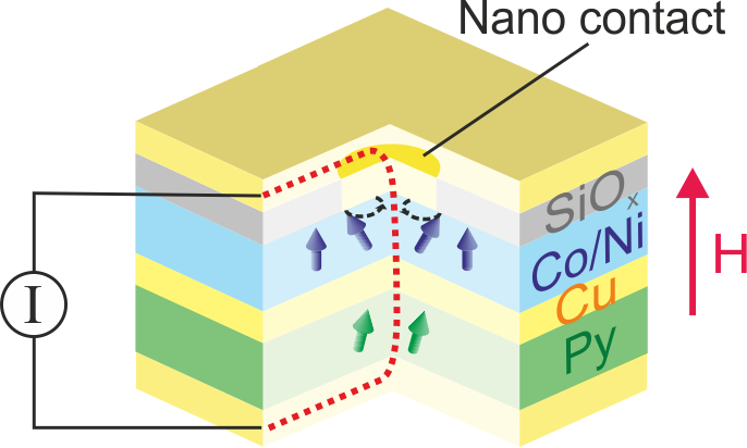
• Spin-torque nano oscillators (STNO)
• Magnetic random access memory (MRAM)
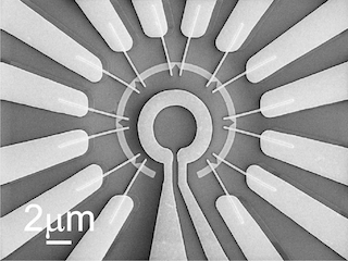
Reducing the dimensionality leads to a plephora of exciting phenomena. The group has extensive experience in nanopatterning techniques, such as electron beam and photo lithography, reactive ion and chemical etching, and ion milling. The range of thin film deposition techniques, mainly for magnetic materials, dielectrics, or contacts, are sputtering, electron gun and thermal evaporation, PECVD, and PLD. We are currently working on processes which allow us to fabricate nanodevices made out of topological materials, such as topolocial insulators.